5-Stage Pipelined RISC-V Processor
RV32I core with hazard detection and forwarding, running at 100 MHz on Artix-7.
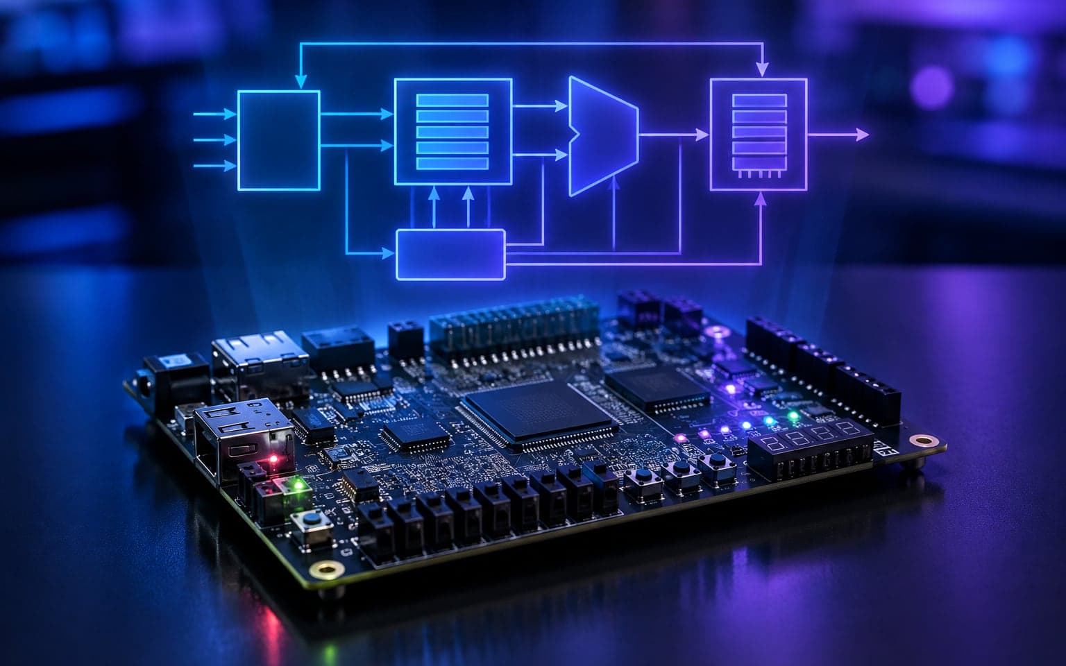
A classic five-stage pipeline (IF, ID, EX, MEM, WB) written in SystemVerilog and implemented on a Nexys A7. It supports the full RV32I instruction set with a hazard unit, data forwarding and pipeline registers, and was verified through simulation and on-board tests. Compared with the single-cycle design it delivers roughly four times the throughput.
README · rendered from GitHub
5-Stage Pipelined RISC-V Processor on FPGA





Project Overview
This project implements a 5-Stage Pipelined RISC-V Processor using SystemVerilog on a Nexys A7 (Artix-7 FPGA). It extends the previous Single-Cycle Processor architecture by introducing instruction-level parallelism through pipelining, dividing instruction execution into five stages Instruction Fetch (IF), Instruction Decode (ID), Execute (EX), Memory Access (MEM), and Write Back (WB). The processor supports the complete RV32I instruction set (R, I, S, B, U, J types), integrates pipeline registers, forwarding logic, and a hazard detection unit to resolve data and control hazards, and achieves significant throughput improvement compared to a single-cycle design.
Tools & Technologies
| Type | Tool / Technology |
|---|---|
| Hardware | Nexys A7 FPGA (Artix-7, Digilent) |
| Language | SystemVerilog (HDL) |
| Software | Xilinx Vivado (Design, Simulation, Synthesis) |
| Extras | RISC-V Assembly, .mem files for memory initialization |
Key Features
System Architecture
Each instruction progresses through five sequential stages, enabling instruction overlap for parallel execution:
- IF – Instruction Fetch: Fetch instruction from instruction memory using PC.
- ID – Instruction Decode: Decode instruction, read registers, generate control signals, and compute immediate.
- EX – Execute: Perform arithmetic/logic operations and calculate branch or memory addresses.
- MEM – Memory Access: Read/write data memory as directed by control signals.
- WB – Write Back: Write results to destination register.
Comparison: Single-Cycle vs Pipelined Architecture
| Feature | Single-Cycle | Pipelined |
|---|---|---|
| Execution Time / Instruction | One long cycle | Five shorter cycles |
| Clock Period | Determined by slowest operation | Reduced (stage-based) |
| Throughput | One instruction at a time | One per cycle (after fill) |
| Latency | 1 cycle / instruction | 5 cycles / instruction |
| Hazard Handling | Not required | Forwarding, stalls, flushes |
| Performance | Moderate | 3–5× higher throughput |
Key Components
- Program Counter (PC): Holds current instruction address and updates sequentially or to branch/jump target.
- Instruction Memory: Stores compiled RISC-V machine code and supplies 32-bit instructions each cycle.
- Control Unit: Decodes opcodes and generates synchronized control signals for all stages.
- Immediate Generator: Extracts and sign-extends immediates for all instruction types.
- Register File: Contains 32 general-purpose registers (x0–x31); supports 2 reads and 1 write per cycle.
- ALU (Arithmetic Logic Unit): Executes arithmetic and logical operations as per ALUOp signals.
- Data Memory: Handles 32-bit load/store operations with aligned access.
- Branch Comparator: Compares register values for conditional branches.
- Pipeline Registers: IF/ID, ID/EX, EX/MEM, MEM/WB — store intermediate data and control signals.
- Forwarding Unit: Bypasses results from EX/MEM or MEM/WB to resolve RAW dependencies.
- Hazard Detection Unit: Inserts stalls or flushes pipeline on load-use or branch hazards.
Implementation
The design follows a modular approach, allowing each component (ALU, Register File, Control Unit, etc.) to be independently tested using SystemVerilog testbenches before integration.
All modules are synthesized in Vivado and integrated in the top.sv module, which handles global clock, reset, and data flow.
Testing & Results
Testing was performed through simulation and FPGA implementation:
- Module-Level Testing: Each unit (ALU, Hazard Unit, Forwarding Logic, etc.) verified individually.
- Integration Testing: Pipeline registers and control paths validated for signal synchronization.
- System-Level Testing: Complete processor executed RISC-V programs for end-to-end verification.
- FPGA Verification: Design successfully implemented on Nexys A7 with 100 MHz clock.
Instruction Testing
| Instruction Type | Examples | Status |
|---|---|---|
| R-Type | add, sub, and, or, slt | Passed |
| I-Type | addi, andi, ori, lw | Passed |
| S-Type | sw | Passed |
| B-Type | beq, bne, blt, bge | Passed |
| U-Type | lui, auipc | Passed |
| J-Type | jal, jalr | Passed |
Performance Analysis
| Metric | Single-Cycle Processor | 5-Stage Pipelined Processor |
|---|---|---|
| Execution Flow | One instruction at a time | Five instructions in parallel |
| Clock Period | Long (slowest path) | Shorter (stage-based) |
| Throughput | 1 instruction / cycle | 1 instruction / short cycle (after fill) |
| Hazard Handling | None required | Forwarding + Stalls + Flush |
| Performance Gain | – | ≈ 4× Improvement |
RTL Diagrams
These RTL (Register-Transfer-Level) views were auto-generated in Vivado to visualize structural connectivity among modules.
RTL schematic of the Top Module
RTL schematic of the Control Unit Module
RTL schematic of the Instruction Memory Module
RTL schematic of the Branch Comparator Module
RTL schematic of the Immediate Generator Module
RTL schematic of the Register File Module
RTL schematic of the Program Counter Module
RTL schematic of the ALU Logic Module
RTL schematic of the Data Memory Module
RTL schematic of the Pipelined Register Module
RTL schematic of the Forwarding Unit Module
RTL schematic of the Hazard Detection Module
Timing Diagrams
Timing waveforms confirm correct overlap of instructions, data forwarding, and stall behavior across pipeline stages.
Timing Diagram of the Top Module
Timing Diagram of the Control Unit Module
Timing Diagram of the Instruction Memory Module
Timing Diagram of the Branch Comparator Module
Timing Diagram of the Immediate Generator Module
Timing Diagram of the Register File Module
Timing Diagram of the Program Counter Module
Timing Diagram of the ALU Logic Module
Timing Diagram of the Data Memory Module
Timing Diagram of the Pipelined Register Module
Timing Diagram of the Forwarding Unit Module
Timing Diagram of the Hazard Detection Module
Conclusion
The 5-Stage Pipelined RISC-V Processor successfully demonstrates a modern pipelined architecture implemented entirely in SystemVerilog and deployed on the Nexys A7 FPGA.
Through instruction-level parallelism, forwarding, and hazard management, the processor achieves a ≈ 4× increase in throughput compared to a single-cycle design while maintaining functional correctness and timing stability at 100 MHz.
Future Enhancements
- Branch Prediction Unit – reduce control hazard penalties.
- Instruction & Data Caches – improve memory latency.
- Out-of-Order Execution – further boost parallelism.
- Exception/Interrupt Handling – add system-level robustness.
- RISC-V Extensions – support M, F, and CSR extensions for advanced features.
License
This project is licensed under the MIT License.
Author
Awais Asghar
NUST Chip Design Centre (NCDC)
Project Folder Structure
Regards
More in FPGA
Related projects
 Private repo
- SystemVerilog
- Vivado
- Vitis HLS
- PyTorch
 Private repoFPGA2026
AI Accelerator: Co-Design Pipeline
The step-by-step hardware-software flow behind the U-Net accelerator on Zybo Z7-20.
- SystemVerilog
- Vitis HLS
- Vivado
- C
- SystemVerilog
- Vivado
- Nexys A7
- Assembly